1. Features of Cat-CVD
Most of industrial consumer products are coated by various thin films.
Some of products may be covered with painting or plating films. Thin film
coating is also seen in modern electronic products. In such cases, quite
often, the quality of coating films decides the performance of the electronic
products themselves. For instance, in liquid crystal display (LCD), transistors
made by semiconductor thin films are working as a key device to control
the brightness and colors of pictures. Ultra-large scale integrated circuits
(ULSI), used in computers, contain so many thin films and the quality of
such thin films decides the performance of ULSI. In solar cells, also,
the quality of thin films determines their energy conversion efficiency.
Thin films used in such electronic products are often required to be prepared
at temperatures as low as 300℃ or less, keeping film quality as high as
possible. The plasma enhanced chemical vapor deposition (PECVD) method,
so far, appears used to obtain thin films satisfying such requirements.
In PECVD, source gases are introduced into a vacuum chamber, where the
molecules of source gases are decomposed by the physical collisions with
energetic electrons generated in plasma, and the decomposed species are
transported to the substrates to form films. This PECVD method is one of
the most successful thin film technologies; however, because of the progress
of industry society, the requirements are getting even severe. In PECVD,
the surfaces of substrates or of previously deposited thin films always
suffer from the damages by the collisions with ions generated in plasma
along with energetic electrons. For the further improvement of performance
of consumer electronic products, this plasma-induced damage becomes a serious
problem in PECVD. Thus, the development of a new method obtaining high
quality thin films at temperatures below 300℃ with no plasma-damages is
strongly required.
Our developed new CVD method, named as Catalytic Chemical Vapor Deposition
(Cat-CVD) method, is to satisfy these requirements. In Cat-CVD, the molecules
of source gases are decomposed in a vacuum chamber by the catalytic cracking
reaction with heated catalyzers, and the cracked species are transported
to the substrates to form films there. In the mechanism of gas decomposition
in Cat-CVD, the films or substrates are free from plasma damages. Since
metal wires are often used as catalyzers, this method is also known as
“Hot-Wire CVD”, or “HWCVD”.
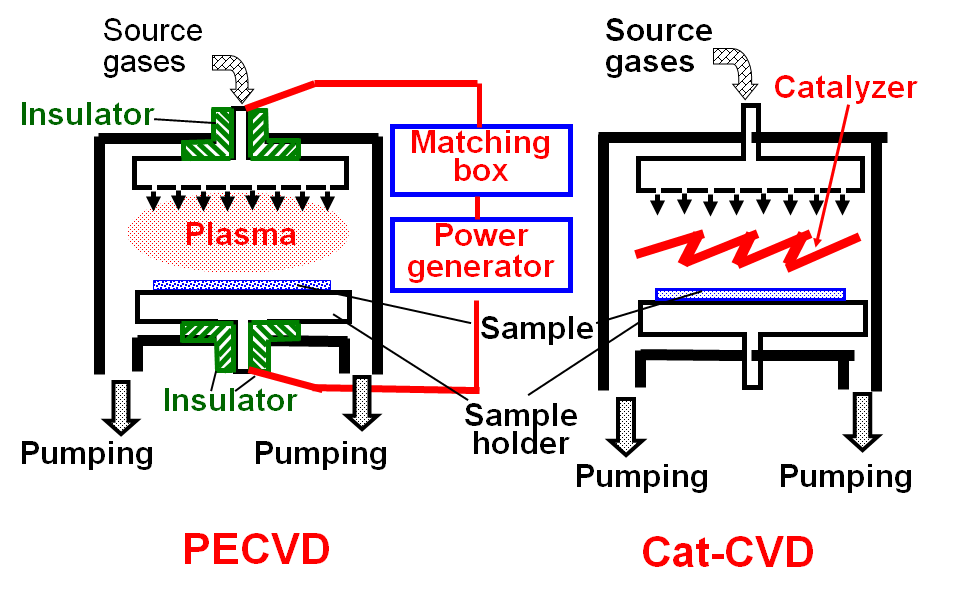
Fig.1 Schematic view of PECVD and Cat-CVD apparatuses.
Figure 1 shows schematic view of PECVD and Cat-CVD apparatuses. In PECVD,
the two parallel electrodes have to be electrically insulated from the
chamber to generate glow discharge between these two electrodes. In most
cases, the glow discharge plasma is excited by radio frequency (RF) alternative
wave of 13.56 MHz, and a matching system to transfer the RF power to the
electrodes has to be equipped, in addition to a RF power generator. Thus,
the system of PECVD is complicated. On the other hand, in Cat-CVD, only
catalyzing wires are installed inside the chamber, and the deposition system
becomes very simple.
Recently, it has been reported that the quality of PECVD films can be
improved by increasing plasma frequency from RF to Very High Frequency
(VHF) range. The increase of plasma frequency makes it even complicated
to adjust the stable plasma generation. Particularly, since the films deposited
on the electrode or other area of the chamber cause the change of plasma
conditions, the chamber has to be cleaned quite often to keep the same
stable plasma. In addition, by increasing plasma frequency, it becomes
even harder to realize uniform film deposition in large area over 1.5 m
square.
There have been so many reports and papers demonstrating promising effects
of the increase of plasma frequency; however, it is not so easy to install
VHF plasma into the mass-production without adapting particular structures
such as ladder electrodes.
Particularly, when the frequency used in mass-production system becomes
higher than 27 MHz, the adjustment of plasma for long times is getting
even more difficult without frequent cleaning. When we introduce VHF plasma
into the mass-production, we have to carefully estimate the film-preparation
cost including cleaning gas cost.
On the other hand, there are substantially the following advantages in
Cat-CVD:
- 1)There is no worry about plasma damage.
- 2)Since there are no special insulators at the electrodes, the mechanical system for mass-production can be easily installed in the substrate holders or other parts.
- 3) Since we need not worry about abnormal glow discharge, the film can be deposited uniformly on the samples with various shapes including sharp edge. This advantage is used to deposit Poly-Tetra-Fluoro-Ethylene (PTFE, or Teflon in commercial name) films on razors to make their surface smooth.
- 4) The cost of apparatus can be lowered in principle, since the deposition system is so simple.
- 5) Large area deposition is easy by simply expanding the spanning area of catalyzing wires.
- 6) When the catalyzing wires are hung vertically, the films are deposited on the both sides of the catalyzer and the productivity becomes double.
Figure 2 demonstrates the images of the interface between amorphous-silicon
(a-Si) and crystalline-silicon (c-Si) observed by the Scanning Transmission
Electron Micro-scope (STEM) with a spatial resolution as high as 0.08 nm.
The figure shows the images of both Cat-CVD a-Si/c-Si interface and PECVD
a-Si/c-Si interface. The STEM machine used here, JEOL JEM-ARM200F, is one
of the top grade experimental equipments possessed by JAIST. The machine
was, used be, the world’s first operating machine. To keep the spatial
resolution of 0.08 nm, the room is specially designed to avoid the vibration
conducted from the land and the vibration made even by the sound or voice
in the room. The room has a heavy concrete floor with a thickness more
than 1 m and all walls are covered with the sound absorbers to be kept
silent.
In this case, the samples are observed from the direction of (110), and
thus, many Si-Si pairs with an atom-distance of 0.15 nm are observed in
c-Si regions as predicted by the crystalline model of c-Si.
In case of Cat-CVD a-Si/c-Si interface, the c-Si image is fading into
a-Si dark image with a transition layer of 0.6 nm, but in case of PECVD,
it is 1.8 nm. In the observation by STEM, the image is drawn by electrons
transmitted through the sample with a thickness of 10 to 20 nm. That is,
the wider transition layer seen in the PECVD a-Si/c-Si interface means
larger fluctuation or roughness at the interface than that in Cat-CVD a-Si/c-Si
interface. The depth of damages created by collisions with Si atoms can
be evaluated theoretically by using the formula of nuclear stopping power
of Si atoms in c-Si. The depth of damages by Si atoms with energy of about
50 eV is estimated to be 1 to 2 nm. The collision energy of 50 eV is quite
common as the energy often seen at the sheath of plasma. In case of PECVD,
it is natural to think that Si atoms at the surface with a layer thickness
of 1 to 2 nm are removed or scattered to make rough surface or interface.
This is the real figure of plasma damages.
This observation has been carried out several times by using PECVD samples
made by outside of JAIST. As a result, it is found that the reproducibility
is very high, and that the transition layer from c-Si to PECVD a-Si is
always 1.8 to 2.0 nm.
So far, the roughness at the interface between PECVD films and c-Si substrates
has been accepted in industry or many cases. However, when really plasma-damage-less
interface is required for achieving top grade device performance, this
difference between Cat-CVD and PECVD interfaces would have serious meaning.
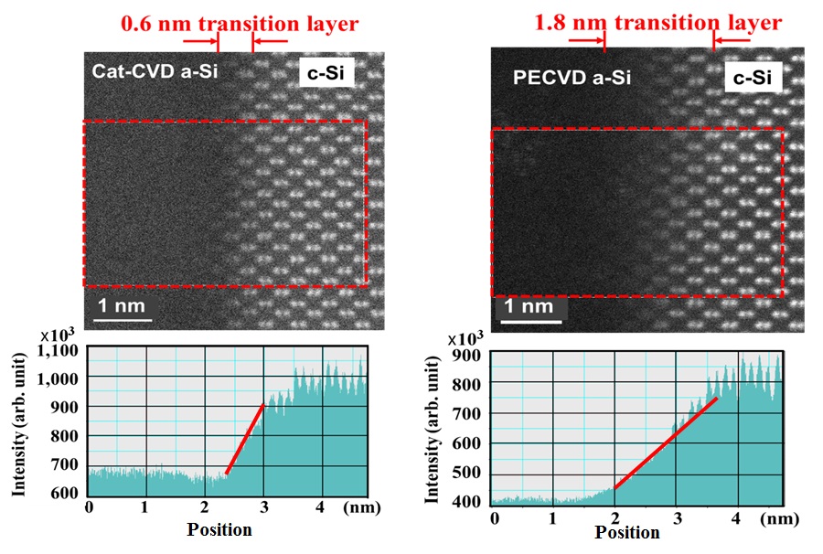
Fig.2 STEM images of Cat-CVD a-Si/c-Si interface (left), and PECVD a-Si/c-Si
interface (right). Intensities from crystalline signals are
also shown in the lower figures.
In addition to this, 5) is also a great advantage in Cat-CVD. In PECVD,
when the deposition area is expanded, as mentioned briefly above, the uniformity
is lost because of generation of standing wave of RF wave. For instance,
the wavelength of 13.56 MHz frequency is about 22 m in a vacuum. The length
between the position of peak power and that of power 0 should be 1/4 of
wavelength, and thus, it is about 5 m. The length is shortened when the
chamber is filled by source gases, since the velocity of electromagnetic
waves decreases in medium. When the size of sample tray is about 2 m in
mass-production system, the value is no longer negligible for uniform deposition.
If the plasma frequency is increased to 60 MHz for improving the film quality,
for instance, it is even harder to realize uniform deposition on large
area. For improvement of productivity for film deposition to reduce the
film preparation cost, large area deposition is inevitable approach. This
is a strong obstacle for PECVD, particularly, for VHF PECVD.
Here, we have to mention some of useful and effective attempts to overcome
the demerit of PECVD. One idea is the introduction of “Hollow-Cathode”
system, carried out in PECVD machine used in fabrication of thin film transistors
of LCD production. In a large electrode-plate, small holes with a diameter
less than 10 mm and a depth about also 10 mm are formed. In such a small
hole, a small gas inlet hole and insulated small electrode are installed.
Glow discharge is generated inside such a small holes. This type of system
is called as “Hollow Cathode”. If such small Hollow Cathodes are arrayed
on the electrode-plate keeping a distance of two Hollow Cathodes at 100
mm or less, large area deposition becomes possible without worry about
standing wave problems, although high level technology is required to keep
uniform glow discharges in many arrayed small Hollow Cathodes. By this
technology, already, the apparatus for 3 m size deposition, so called “10th
generation PECVD machine”, has been installed in LCD industry.
Even in this case, keeping plasma stably is still a big issue. When films
are deposited near electrodes at Hollow Cathodes, plasma conditions are
changed. Thus, the frequent cleaning of the chamber and also of the areas
near electrodes are necessary. In the mass-production system, the etching
gases such as nitrogen tri-fluoride (NF3) are excited by microwave-plasma
at the outside of the chamber and such excited species are introduced into
the Hollow Cathodes through gas inlet holes, in order to clean up the Hollow
Cathodes and the area surrounding them. This production system is quite
successful in LCD industry; however, it should be noticed that the cost
of NF3 is not negligible. In addition, when we use halogen gas such as
NF3, vacuum system should be prepared for it. All these things are reason
for cost increase in this system. In case of LCD industry, the increase
in cost can be absorbed by mixing with other costs. However, in solar cell
industry, that should be difficult since further lowering the production
cost is always required.
Please notice that there are no worries about constructing such complicated
and expensive systems in Cat-CVD.
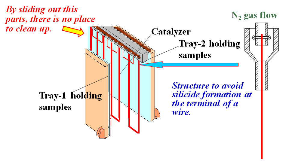
Fig.3 Schematic view of vertical type Cat-CVD apparatus. This system is used in large area mass-production machines.
Figure 3 shows schematic view of the Cat-CVD apparatus with catalyzers
hung vertically in the deposition chamber, as mentioned at above 6). Here,
two sample trays are set in parallel at the both sides of hanging catalyzing
wires. After a-Si films are deposited for more than 1 month continuously,
the hanging parts of catalyzing wires and the mechanical parts for moving
trays are all slid out from the deposition chamber for chemical cleaning
carried out at elsewhere outside of the chamber. The same parts which have
been cleaned up are re-used and newly set at the top of the chamber. Since
the most of areas inside chamber are all covered with trays, there is no
place of chamber cleaning. We need not to use halogen gas at all and cleaning
frequency is very low. This is one of the big advantages in Cat-CVD.
Apart from 6 advantages described above, there is one more important advantage in Cat-CVD.
7) The efficiency of source gas use is by 5 to 10 times higher than that
of the conventional PECVD.
In PECVD, molecules of source gases are decomposed by the physical collisions
with energetic electrons. This means that the collisions of a point with
another point in 3-dimensional space occur in PECVD as illustrated in Fig.
4, left. The probability of such collisions is not so high, and some of
molecules are evacuated without any collisions. On the other hand, in Cat-CVD,
molecules are collided with 2-dimensional solid surface; the collisions
of a point with 2-dimenasional area is utilized as shown in Fig.4, right.
The probability of the collisions becomes high and in general deposition
conditions a molecules is collided with the surface of catalyzer by more
than 10 times before evacuation. Thus, the efficiency of gas use in Cat-CVD
becomes much higher than that of PECVD.
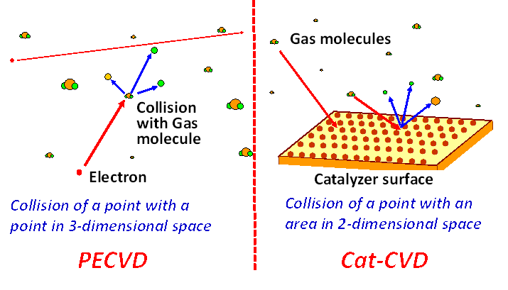
Fig.4 Collisions in PECVD (left) and in Cat-CVD (right)
The data of gas efficiency in factory is not open in any companies. However,
it is guessed that the gas efficiency in PECVD is only several % to obtain
high quality films with a cost-effective deposition rate, but that the
gas efficiency in Cat-CVD reaches to 30 % or more. In addition, the films
with same quality to PECVD films are obtained with almost double the deposition
rates in case of Cat-CVD.
When the saline (SiH4) gas is used as a source gas particularly for large
area deposition, this advantage of high efficiency of gas use becomes more
remarkable. The volume of exhaust gas after deposition can be reduced and
the amounts of dangerous SiH4 gas storage in factory can be also much reduced.
These advantages make the film deposition cost low. The superiority of
Cat-CVD to PECVD appears clear particularly when large area deposition
is carried out without any plasma damages.
2. Reactions on Surface of Catalyzer
Next, let’s consider what happened in the surface of catalyzer. Although there are various cases for the reactions of gas molecules with the surface of catalyzer, here, at first, we like to concentrate on the decomposition of SiH4 molecules with tungsten (W) catalyzer for simple explanation. When a gas molecule reaches at the surface of catalyzer, two types of reactions
are expected. One is that the molecule connects with atoms of catalyzer
surface by physical-adsorption. The other is that the molecule makes a
bond with an atom at the catalyzer surface, by chemical adsorption. In
some probabilities, physically adsorbed molecules are converted to chemical-adsorbed
ones, although the most of physically adsorbed molecules are desorbed.
Let’s consider the case when a molecule approaches into a certain distance
from the surface of catalyzer. If the sum of the energy of a molecule and
the energy of atoms at the catalyzer is larger than the total energy of
bonds formed with decomposed molecules and catalyzer atoms, the molecule
is likely to be decomposed to lower the total energy of the system and
the dissociative adsorption is constructed with catalyzer atoms.
Figure 5 shows illustration of this dissociative adsorption of SiH4 with
W catalyzer for catalyzer temperatures at room temperature (RT) (left)
and at over 1,000℃ (right).
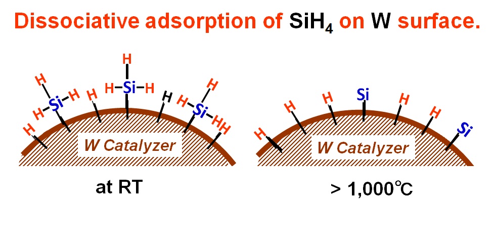
Fig. 5 Schematic illustration of chemical dissociative adsorption for SiH4 and W catalyzer system. The temperature of catalyzer is room temperature (RT) (left) and over 1,000℃ (right).
When a SiH4 molecule approaches to the surface of W catalyzer, even at
RT, it is decomposed as SiH4→SiH3+H, to form W-SiH3 and W-H bonds. That
is, we have to notice that the decomposition of SiH4 is not happened by
the heat but by chemically controlled dissociative adsorption.
This is a story when the catalyzer temperature is RT. Then, when it is
elevated, how does it changes? When the catalyzer temperature is elevated,
the W-SiH3 bond starts to vibrate strongly. However, because of the strong
binding of W-Si, most of SiH3 remains on the surface with large vibration
amplitude. Finally, H atoms in SiH3 are reaching to other W atoms and SiH3
is decomposed to make W-H bonds. It is believed that this happens when
the catalyzer temperatures exceeds over 1,000℃. That is, when the catalyzer
temperature exceeds over 1,000℃, SiH4 is adsorbed with a configuration
of W-Si and 4(W-H) bonds using totally 5 sites on W catalyzer. In other
words, when the catalyzer temperature is higher than 1,000℃, SiH4 cannot
exist on the W catalyzer surface without forming W-Si and 4 of W-H bonds.
The bond configuration of dissociative adsorption is determined by the
type of molecule and catalyzer materials. In the case of SiH4, as mentioned
above, W-Si and W-H is the final form. However, for instance, in case of
decomposition of ammonia (NH3), after forming W-NH2 and W-H, NH2 cannot
stay on the W catalyzer anymore and desorbs from the catalyzer to supply
H and NH2 in space. Decomposition of NH3 needs only 2 sites on W catalyzer.
The bond configuration is determined by how long dissociative adsorption
can be hold keeping adsorbed states.
When W-H and W-Si bonds are formed at over 1,000℃, H atoms are soon desorbed
into the chamber; however, the most of Si atoms are likely to remain on
W surface. If a Si atom remains on W surface for a certain time which is
enough to form many W-Si bonds around the first single W-Si bond, and if
the number of W-Si bonds exceeds the critical threshold size for forming
a silicide block, a part of W surface is covered with silicide. To avoid
it, the temperature of catalyzer has to be even more elevated over 1,750
to 1,800℃. This is the reason why the catalyzer temperatures should be
elevated over 1,750℃ in case when a-Si films are obtained by Cat-CVD from
SiH4 gas with W catalyzer. The heat is not used for decomposition of SiH4,
but used only for avoiding silicide formation. Actually, when Tantalum
(Ta) is used instead of W as the catalyzer, the temperature can be lowered
by about 100℃ from the temperature of W catalyzer. For such a reason, in
mass-production systems to prepare a-Si films by Cat-CVD, Ta catalyzers
are widely used instead of W catalyzer.
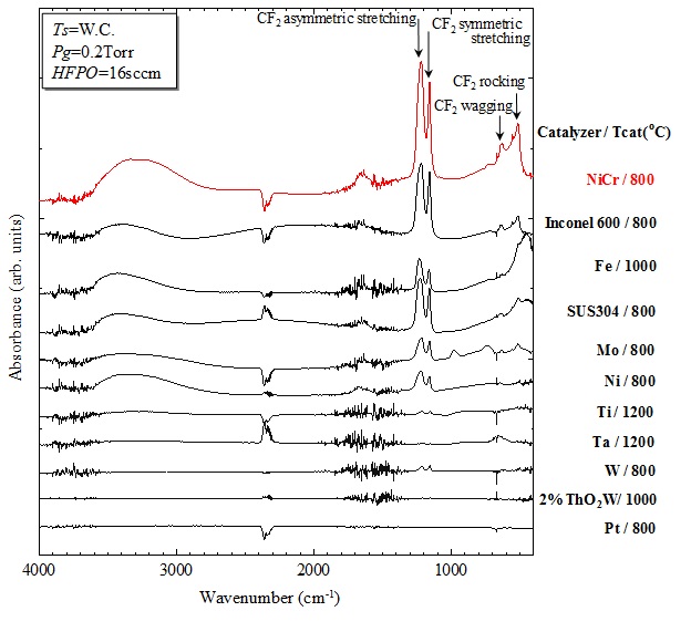
Fig.6 Infrared absorption spectra of PTFE films prepared by Cat-CVD from HFPO with various catalyzing materials and temperatures, The peak height of infrared absorption peaks simply corresponds to the film thickness.
The story mentioned above is just for explanation of a-Si film deposition.
If we change the story for the deposition of PTFE films, relationship between
catalyzer and source gas will becomes even clearer.
Next, let’s consider the case of deposition of PTFE (Teflon) films from
HFPO (Hexa-Fluoro-Propylene-Oxide) gas by Cat-CVD. Figure 6 shows the infrared
absorption spectra of PTFE films which are prepared from HFPO gas but with
various catalyzing metal wires. In the figure, the catalyzers and their
temperatures during the deposition are described. This figure simply shows
the infrared absorption spectra of various films prepared with the same
deposition times. The peak height simply corresponds to the thickness of
deposited films with the same deposition times. That is, the figure simply
shows the deposition rates of PTFE films when various catalyzing materials
are used.
At first, from the figure, it should be noted that the deposition rates
depend on catalyzing materials but not on the temperatures of catalyzer.
It is found that PTFE films are easily obtained with larger deposition
rates when Nichrome (NiCr), Inconel (commercial name of Nichel (Ni) containing
special metal alloys produced by Special Metals Corp.) and Stainless-Steel
(SUS) are used as catalyzers. These materials contain Ni atoms. That is,
when Catalyzer includes Ni atoms, the deposition rate appears to increase.
Interesting phenomena can be seen in the figure. When a pure Ni wire is
used, the deposition rate is not so faster than that obtained by Ni alloys.
This suggests that Ni atoms are essentially needed, but other different
atoms are also required probably for reducing the energy for dissociative
adsorption of HFPO molecule.
Figure 7 demonstrates our one speculation for the dissociative adsorption
of HFPO on NiCr catalyzer, for better understanding of the phenomena, although
there have not been verified at all at the moment. At first, just for explanation
of image, HFPO, F3C-FC-O-CF2, is assumed to be dissociatively adsorbed
as configuration of Ni-CF3 and Cr-FC-O-CF2. Here, if other metal atom such
as Chromium (Cr) is better to make bond with –FC-O-CF2 than Ni, NiCr is
better catalyzer than pure Ni. Although it is widely known that HFPO, F3C-FC-O-CF2,
is usually decomposed to F3C-(=O)-CF + CF2, we do not know at the moment
how such decomposed configuration changes when catalyzing metals exist
near HFPO. Please understand that this explanation is completely based
on imagination.
Anyway, this demonstrates that the decomposition of source gas molecule
is completely depending on the reaction at the surface of the catalyzer
and not depending on only heat. This is the reason why we use the term
of “Cat-CVD” instead of simple “Hot-Wire CVD”, “Hot Filament CVD” or other
terms.
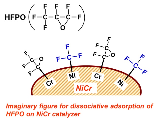
Fig.7 An imaginary drawing of dissociative adsorption of HFPO on NiCr catalyzer.
Figure 8 demonstrates the movie showing a drop of water on SUS substrates
coated with PTFE by Cat-CVD (left) and without PTFE (right), and Fig.9
demonstrates another movie showing a drop of water on cotton with PTFE
coated by Cat-CVD and without coating of PTFE.
Recently, Cat-CVD technology has been expanding to prepare high quality
organic films. This area appears promising for future development.