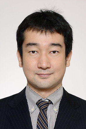
Explore crystal growth mechanism through in-situ observation
Laboratory on Next-Generation Silicon Photovoltaics
Senior Lecturer:MAEDA Kensaku
E-mail:
[Research areas]
Crystal Growth, Solar cells, Nonlinear optics
[Keywords]
in-situ observation, grain boundary, twinned crystal
Skills and background we are looking for in prospective students
Students are preferred to have basic knowledge of physics and mathematics.
An attitude of impartial evaluation of experimental results is also required.
What you can expect to learn in this laboratory
Students can achieve skills in the operation of experimental setup, gas control system, heating system and microscope, and date collection and analysis methods. Communication and problem-solving skills are developed through weekly seminar activities and daily discussions.
New discoveries often come from failed experiments. I hope that students will develop skills that will be useful when they join a company after graduation, such as the ability to carefully read features that would normally go unnoticed and the ability to think things through rationally.
【Job category of graduates】 Manufacture and research work of electronics and materials related companies
Research outline
To advance the development of electronics and opto- electronics, it is essential to improve the quality of the crystals used as materials. Crystals are solids with regularly arranged atoms, which are formed by growth from an ambient phase. This growth process is important for obtaining high performance crystals. By carefully observing the growth process, the mechanisms are elucidated and technologies for growing high performance crystals are developed.
1.In-situ observation of the formation process of thin-film polycrystalline silicon
The semiconductor silicon is widely used as substrate for solar cells. Thin-film polycrystalline silicon can be made by exposing amorphous silicon on a glass substrate to pulsed light (flashlamp annealing light), which is superior in terms of productivity and cost to crystalline substrates made by slicing Si ingot. By observing the process of polycrystallisation of amorphous silicon, the formation mechanism of the structure that causes the degradation of solar cells can be clarified, and technologies to suppress its formation will be developed.
2.Fabrication of laser wavelength conversion device (periodic twin crystal)
Ultra-fine semiconductor lithography and laser processing require shorter wavelengths from all-solid-state laser sources. All-solid-state lasers can be realised by wavelength conversion of a solid-state laser using a nonlinear optical crystal, which is more stable and compact than using gas as a laser source.
The conversion efficiency can be improved by forming a periodic structure in the nonlinear optical crystal, which is produced by applying an external electric field to ferroelectric crystals. In this study, to introduce periodic structure in non-ferroelectrics, we are developing an inversion technique using twinning formation.
3.Observation of the growth process of compound semiconductors
Single crystalline silicon is widely produced worldwide as a substrate material for semiconductor devices. Compound semiconductors (InSb, GaSb, GaAs, etc.) are produced in smaller quantities, but these crystals are indispensable for the future development of electronics and the development of single crystal growth technology is important. The aim is to observe how crystals grow and to understand how defects such as twins and grain boundaries are formed.
Key publications
- K. Hu, K. Maeda, H. Morito, K. Shiga, K. Fujiwara, In situ observation of grain-boundary development from a facet-facet groove during solidification of silicon, Acta Materialia, 153, 186(2018).
- K. Maeda, A. Niitsu, H. Morito, K. Shiga, K. Fujiwara, In situ observation of grain boundary groove at the crystal/melt interface in Cu, Scripta Materialia, 146, 169(2018).
- K. Maeda, S. Uda, K. Fujiwara, J. Nozawa, H. Koizumi, S. Sato, Y. Kozawa, T. Nakamura, Fabrication of Quasi-Phase-Matching Structure during Paraelectric Borate Crystal Growth, Applied Physics Express, 6, 15501(2013).
Teaching policy
Our group has a policy of supporting students’ individual initiatives, and their own ideas can be included in their research. A morning meeting is held every weekday, and the activities of each student are shared. Students can also have simple research discussions in the meeting. In a study meeting, held every Saturday, a duty student is required to explain the detail of a journal paper and to answer questions from other students and staffs, by which students can obtain high basic academic skills. Students can actively present their research achievements, and acquire ability to write their own research paper for themselves.
[Website] URL:https://www.jaist.ac.jp/ms/labs/ohdaira/en/home_e